
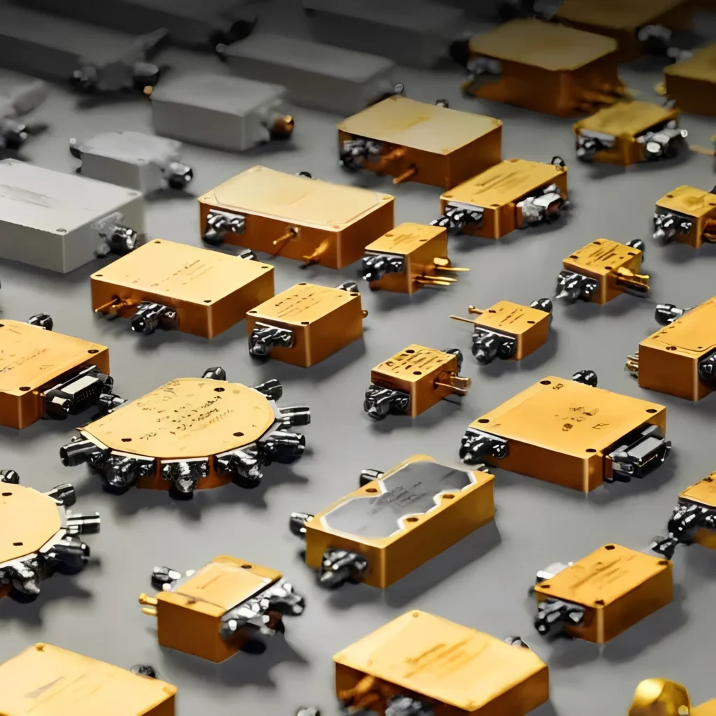
I often see a system team blame the RF power amplifier first. The link drops. The PA gets hot. The output power falls. Then the project slows down fast.
RF power amplifiers work by using a biased active device to turn a small RF input into a larger voltage and current swing at the output, but in modern systems the real “work” is balancing linearity, efficiency, heat, matching, and protection so the amplifier can run in your system for a long time.
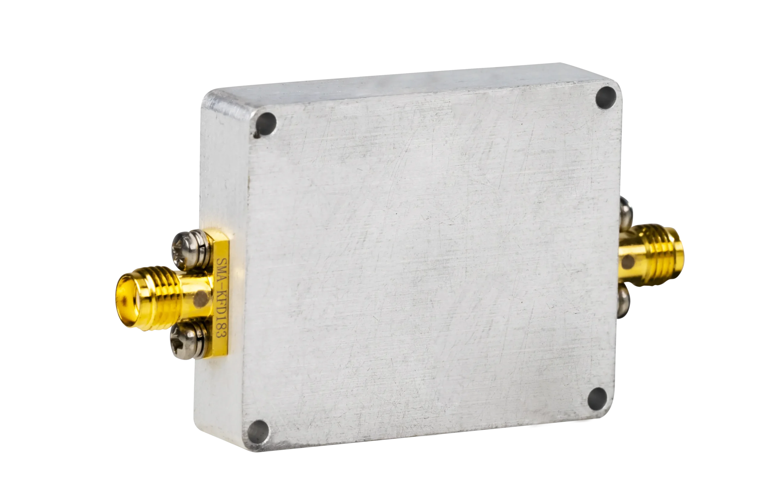
I do not treat a power amplifier as a simple “gain block.” I treat it as a machine that makes the signal stronger and makes the risk larger at the same time. If I want stable output power in the field, I must understand what pushes the PA into compression, what makes it heat up, what triggers protection, and what causes distortion under real modulation.
How to define RF power amplifier requirements?
Many teams start with one sentence: “I need 100 W.” I understand why. It is simple. But it is not enough. In the factory, a single missing detail can make the whole design point wrong. I have seen customers receive a PA that meets the datasheet and still fails their system test, because the requirement was not defined at the same operating point.
I define RF power amplifier requirements by first stating the signal type and operating state (small-signal, linear backed-off, or near saturation), then setting frequency, power, and linearity targets, and finally adding the real system limits like temperature, VSWR, duty cycle, and protection behavior.
I start from the “power type” and the real operating state
The first requirement I lock is not topology. It is the power definition.
- CW power: stable continuous output. This is the hardest on heat.
- Average power for modulated signals: this drives thermal design and reliability. It also links to PAR (peak-to-average ratio).
- Peak or pulse power: this depends on pulse width, duty cycle, and droop limits.
Then I define where the amplifier will run:
- Small-signal region: gain is stable, distortion is low.
- Compression region (near P1dB): gain starts to drop and distortion rises.
- Saturation (Psat): output cannot increase much, efficiency improves, but distortion is strong.
In LTE/5G/OFDM, many systems do not run at pure saturation for long. They run backed off to meet ACLR/EVM. If someone only specifies Psat, I already know we might pick the wrong PA for a comms system.
I write the requirement as a set of constraints, not a single number
Here is the structure I use in real projects.
| Requirement item | What I specify | Why I specify it |
|---|---|---|
| Frequency band | start/stop, key points | gain and match shift with frequency |
| Output power target | CW / average / peak + time | “100 W” can mean three different things |
| Linearity | ACLR, EVM, IMD, P1dB | defines usable power for modulated signals |
| Efficiency | PAE or DC power limit | links to heat and power supply sizing |
| Thermal | baseplate temp, ambient, airflow | prevents field derating surprises |
| Load match | VSWR limit, reflection tolerance | high VSWR can kill or fold back power |
| Duty / burst profile | duty, burst length, PRF | changes junction heating and droop |
| Size and weight | outline + connector rules | impacts mechanical integration |
| Protection behavior | what happens at fault | explains “why output drops” in the field |
I ask the customer the questions that save the most time
When someone tells me “I need 100 W,” I ask:
- Is it CW, average (modulated), or peak?
- What is the highest frequency?
- What linearity target do you need (ACLR/EVM/IMD)?
- What is the worst-case ambient temperature?
- What VSWR can the load reach?
- Do you accept derating or do you need hard power hold?
This is not sales. This is how I stop wrong designs early.
A short personal story I often tell
I once supported a system that “needed 100 W.” The customer meant 100 W peak in short bursts. We built for 100 W CW margin. The PA ran hot, oversized, and expensive. The lesson was simple: a correct PA starts with a correct requirement, not a big number.
How to choose the right device and topology for an RF power amplifier?
A lot of people think device choice is the main secret. I get it. It feels like the fastest path: pick GaN, pick a transistor, and move on. But in practice, topology and matching can make the same device look completely different. I have seen the same transistor produce great results in one design and fail in another.
I choose the right device and topology by matching the system priority (linearity vs efficiency vs bandwidth), then selecting a device technology that supports the voltage, current, and frequency, and finally choosing a topology that meets power and matching needs with stable operation under VSWR and temperature.
I pick based on “what matters most in your system”
In modern RF systems, I see three common priority patterns:
1) Comms systems (LTE/5G/OFDM)
- Linearity targets are strict (ACLR/EVM).
- Efficiency still matters because heat is the enemy.
- The PA often runs backed off.
2) Radar and pulse systems
- Peak power and pulse repeatability matter.
- The PA may run near saturation during pulses.
- Robustness under mismatch is critical.
3) Test and measurement
- Flatness and repeatability matter.
- Calibration and protection behavior matter.
- Clean harmonics and predictable gain curves matter.
Once I know which pattern applies, device choice becomes clearer.
I pick device technology by voltage, frequency, and ruggedness
I keep the device conversation simple in daily work:
- If I need high power density and good efficiency, I often look at GaN options.
- If I need very clean linear behavior at lower power, I may consider other solutions depending on band and budget.
But the real message I tell customers is this: the device does not rescue a weak system definition. I still need clear requirements first.
I choose topology based on power level and bandwidth
Topology is not just an academic topic. It changes matching difficulty and harmonic behavior.
Common topologies I choose from:
- Single-ended: simpler, often fine for moderate power.
- Push-pull: helps even-order harmonics and can improve linearity in some cases.
- Balanced: improves match stability and VSWR tolerance, but adds loss and cost.
- Doherty: often used when efficiency at back-off matters, common in modern comms.
- Distributed / broadband approaches: used when bandwidth is wide, but design becomes harder.
I do not pick “the most advanced” topology. I pick the one that fits the system priority and manufacturing risk.
Matching network is the “gearbox” of the PA
Many customers think the transistor is the PA. In high-power work, the matching network is often the real soul.
The matching network:
- transforms the device’s optimum load to a 50 Ω system
- shapes bandwidth and gain flatness
- controls harmonics and stability
- influences efficiency and thermal stress
So when someone compares two PAs by transistor model only, I warn them: two designs can share the same device and still behave very differently.
A decision table I use in meetings
| System goal | What I often lean toward | Why |
|---|---|---|
| Best linearity | more conservative bias + linear-friendly topology | reduces distortion |
| Best efficiency | topology that supports high PAE | lowers heat and DC power |
| Wide bandwidth | broadband matching approach | keeps gain across band |
| High mismatch survival | balanced ideas + protection | keeps PA alive in the field |
| Dense product | compact layout + controlled thermal path | avoids derating |
How to design an RF power amplifier circuit step by step?
Some people want a “cookbook.” I understand that. But power amplifier design has traps. If I rush, I can get a PA that works on a bench and fails in a cabinet. So I follow a step-by-step flow that forces me to address heat, stability, matching, and protection early.
I design an RF power amplifier circuit step by step by locking requirements first, selecting the device and bias, designing input/output matching, verifying stability and linearity across conditions, then building a testable layout with thermal design and protection so the PA can survive real VSWR and temperature.
Step 1: I freeze the “operating point” in words and numbers
I define:
- band and frequency points
- power type (CW/average/peak) and duty profile
- target linearity (if needed)
- target efficiency
- temperature range
- allowed VSWR and fault behavior
If I do not freeze this, I will redesign later.
Step 2: I choose the bias plan and define safe limits
Bias is not a small detail. Bias defines:
- the region of operation
- the idle current
- the thermal baseline
- the linearity behavior
I also set safe limits:
- maximum drain voltage
- current limit
- gate protection
- expected thermal resistance path
Step 3: I design the matching networks as the main product
I treat matching as a system, not as a few components.
Input matching goals:
- stable gain
- good input return loss
- stable under temperature
Output matching goals:
- correct load transformation
- stable output return loss
- harmonic control
- safe operation under mismatch
If I need wideband behavior, the matching network becomes the hardest part. If I need high power, the matching network must handle current and heat.
Step 4: I run stability checks across frequency and conditions
I do not only check stability at the band of interest. I also check:
- low frequency stability (where oscillation can hide)
- out-of-band stability at higher frequencies
- stability under different load impedances
In the factory, instability is expensive. It can burn devices. It can create random failures.
Step 5: I plan thermal and mechanical design early
If the PA must run CW, thermal is not optional.
I plan:
- baseplate, heat spreader, or flange strategy
- mounting torque and flatness rules
- airflow or conduction path assumptions
- where temperature is measured in test
Many “it worked yesterday” failures are thermal drift and protection events.
Step 6: I add protection and control on purpose
Modern PAs are not “naked.” They are controlled.
I consider:
- over-temperature derating
- over-current protection
- over-voltage protection
- reflected power or high VSWR protection
- input overdrive protection
This is often why a customer sees 70 W from a 100 W PA. The PA is not lying. It is protecting itself.
Step 7: I build a test plan that matches how the system will use it
I test:
- gain and output power vs input drive (to see compression)
- P1dB and Psat
- ACLR/EVM if modulated
- efficiency and current draw
- VSWR tolerance and reflection behavior
- thermal soak results (time at power)
Here is the test log structure I like:
| Test item | What I record | Why |
|---|---|---|
| Pin / Pout sweep | curves, not single points | shows compression behavior |
| P1dB / Psat | power and gain at those points | prevents confusion about “gain” |
| Efficiency | PAE or DC input | links to heat |
| Temperature | baseplate and ambient | explains derating |
| VSWR stress | load mismatch cases | validates survival |
| Linearity | ACLR/EVM/IMD | validates comms use |
A personal note about “step-by-step”
When I follow this flow, I avoid the most painful situation: a PA that meets power on a bench but fails in the customer system. That failure usually comes from mismatch, thermal, or protection behavior that was never defined and never tested.
How does amplifier class (A, AB, B) affect RF power amplifier design?
People often ask about amplifier class as if it is a label that decides everything. In real work, class is a bias and conduction choice that pushes the design toward linearity or efficiency. It also changes heat and distortion behavior.
Amplifier class affects RF PA design by changing device conduction angle and bias point, which shifts the trade between linearity and efficiency: Class A is most linear but hottest, Class B is more efficient but more distorted, and Class AB sits in the middle and is common in practical RF power amplifiers.
I explain class in the simplest way I can
- Class A: device conducts for the full cycle. I get strong linearity. I also get high DC power draw and heat.
- Class B: device conducts about half the cycle. I get better efficiency. I also get more distortion and crossover issues.
- Class AB: device conducts more than half but less than full. I get a balance. This is a common practical choice.
I avoid long theory in a practical guide. I focus on what changes in real systems.
Why class matters more in modulated systems
In modern comms signals, the PA sees high peaks and long average power. If I bias too aggressively for linearity, heat becomes my limiting factor. If I bias for efficiency without system compensation, linearity can fail.
So the real question is not “which class is best.” The real question is:
- Do I need strict ACLR/EVM?
- Do I have DPD or system correction?
- How much heat can my enclosure remove?
A simple trade table I use for quick alignment
| Class | What I gain | What I pay |
|---|---|---|
| A | best linearity, simple behavior | highest heat, lower efficiency |
| AB | balanced linearity and efficiency | still needs careful bias control |
| B | better efficiency at power | more distortion, harder linear targets |
Bias and temperature drift are not side topics
Bias is a living parameter. Temperature changes device behavior. If bias control is weak, a PA can shift:
- linearity can degrade
- gain can drift
- protection can trigger earlier
So in the factory, I also care about:
- bias stability vs temperature
- repeatability across units
- how bias is measured and adjusted
The “class” label is not the whole design
Two Class AB amplifiers can behave very differently because of:
- matching network design
- harmonic tuning
- layout and grounding
- thermal path quality
- protection thresholds
So I treat class as one lever, not the full answer.
Conclusion
I see RF power amplifiers as signal boosters and risk concentrators, so I define requirements first, then choose device, bias, matching, and protection to keep linearity, heat, and stability under control in real systems.
Discussion